 The Single PhOton Calibration Stand at KIT, SPOCK, is build to characterize all kind of photosensors like PMTs or SiPMs with highest precision. It consists of a reference light source capable of emitting single photons per pulse, photon shielding and the read-out electronics.
Calibration Setup
Below a schematic view of the setup inside the photon shielding is shown. The integrating sphere is a Labsphere 3P-GPS-053-SL and as photo diode a OSI Opto-electronics UV-100 is used.
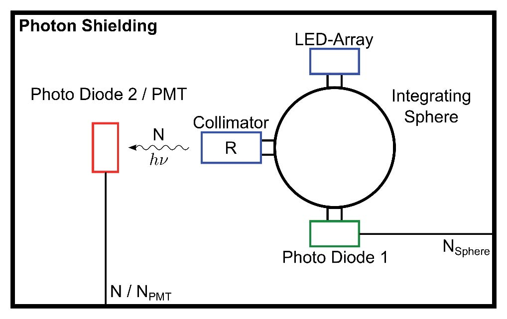
The photon shielding is a wooden box covered on the inside with black flock paper. On the left side of the wooden box is an aluminum panel with connectors serving as feed-through for the voltage supply and the signals. Inside the photon shielding box, the reference light source is located which consists of an integrating sphere, an LED-array, a NIST 1 -calibrated photo diode (Photo Diode 1) and a collimator.
A range of different PVC-collimators is available. The collimator ratio can be measured with a second photo diode placed in front of the collimator. Also different LED-arrays are available (371 nm, 376 nm, 395 nm and 423 nm) equipped with both, continuous and pulsed light sources. The first is used for the collimator ratio measurement while the second is used for SiPM characterization.
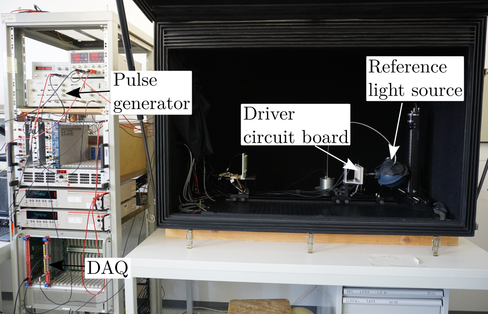
For the future a "Cold-SPOCK" is planned with the option of measuring down to temperatures of -70°C.
Set-Up for SiPM characterization
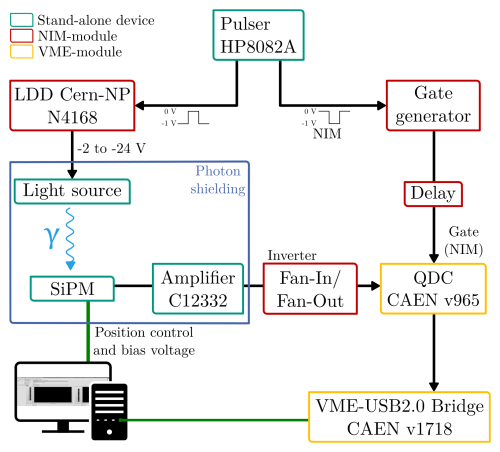
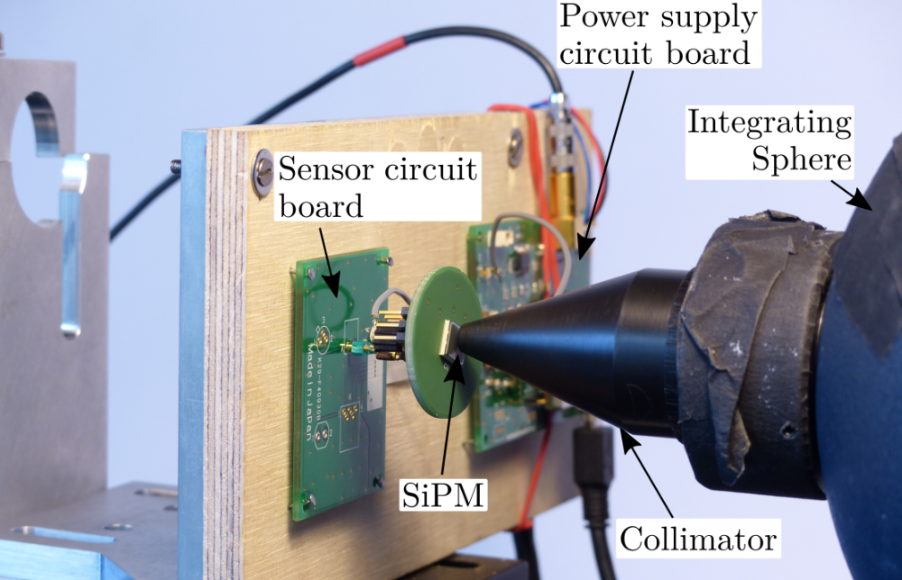
The pulser HP8082A generates a NIM pulse and an inverted NIM pulse. The inverted NIM pulse is passed to the Light Diode Driver (LDD) Cern-NP N4168 which drives the pulsed LED and allows the adjustment of the power emitted by the LED. When the photons of the LED hit the SiPM a output current signal is generated. The SiPM signal is amplified and inverted on a modified Hamamatsu driver circuit board C12332-01. To tell the QDC when to start and stop integrating the SiPM signal a gate signal is used. The QDC is read out by a LabView program.
Example of experimental results
The results shown in the two plots below are obtained for the Hamamatsu UV-light enhanced 64-channel SiPM array of the newest generation (S13361-3050AS-08) and are also published in this article.
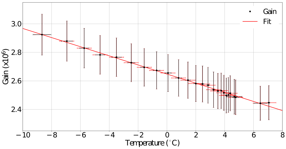
Temperature dependent measurement of the gain. The bias voltage was kept constant at 55.2 V. Statistical errors are shown in black, systematic errors are shown in red.1
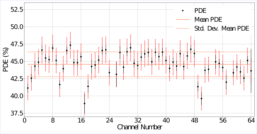
PDE measurement of SiPM array S13361-3050AS-08. The bias voltage was 55.2 V and the incident light had a wavelength of (423 ± 8) nm. The ambient temperature during the measurement was (19.5 ± 1)°C. Statistical errors are shown in black, systematic errors are shown in red.1
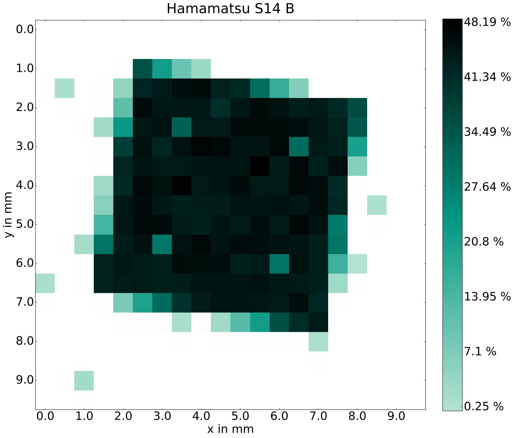
PDE scan of Hamamatsu Photonics S14 SiPM with 6x6 mm2 active area measured at 3 V overvoltage. Overall the PDE is homogeneous in the active area of the SiPM. At the edges the measured PDE is lower since there not all photons hit the active area. The four spots with lower PDE are the positions where the connectors are placed.
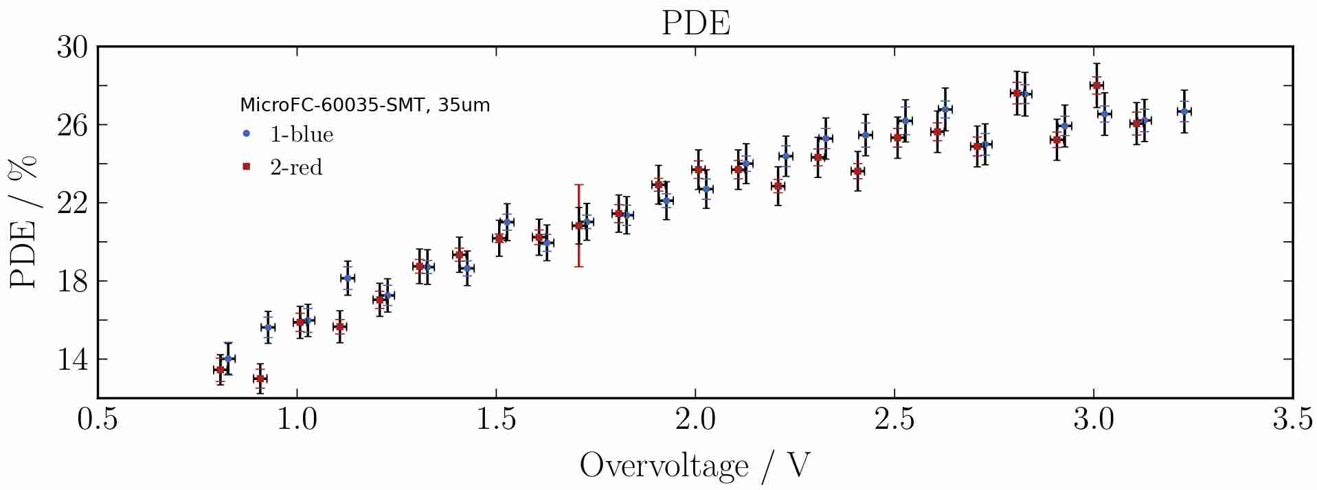
PDE of the SensL SiPM. The statistical errors are plotted in color and the systematic errors in black. The shape of the curves is as expected. The PDE reaches a maximum value of (27.56 ± 0.48 stat ± 1.12 sys)% at (2.83 ± 0.02)V overvoltage for 1-blue and (28.00 ± 0.44 stat ± 1.13 sys)% at (3.01 ± 0.02)V overvoltage for 2-red.
Contact
Karlsruhe Institute for Technologie
Institut für Kernphysik
This email address is being protected from spambots. You need JavaScript enabled to view it.
Phone nr : +49 721 608 22284
1 from M.Renschler et al., Characterization of Hamamatsu 64-channel TSV SiPMs, NIM A, Volume 888, 2018, https://doi.org/10.1016/j.nima.2018.01.029